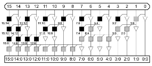
The term "divide-and-conquer tree" also applies to the Sklansky adder. The minimum depth prefix network provided by Sklansky’s (1960) conditionally sum of addition logic for prefix addition will comes in the expense of increasing the fan-outs in some computational nodes. The longest lateral fanning wires extend outward from a node to n/2 additional nodes . Large amounts of latency are accounted for by the Sklansky’s adder’s fan-outs, which will see a significant increase in both the critical path and in-puts to outputs. When the adder’s bit count increases, this results in a decrease in the structure’s performance. Therefore, The no of computational nodes is indicated as [n/2.(log2(n))] .
This adder have been designed using the Verilog Hardware Description Language using Xilinx.ISE.Navigator.10.1 software, and modelsim.6.5e was used for all simulations. It is analysed and compared to determine how the proposed adders perform. The implementation code for 16-bit Sklansky Adder was developed in this proposed architecture, and delay and area values have been observed . The correlation of adders is the major element in the trade-off between these various topologies. These simulated output wave forms and RTL schematics have been generated and synthesis is carried out by chipscope. OpenLANE and Caravel are used with Skywater 130nm PDK. OpenLANE flow consists of multiple itersative stages where we obtain GDSII form RTL netlist. This chip design acquired from OpenLANE is used in caravel to place it on an SoC and design is hardened by placing our HDL code in user_project_wrapper and user_proj_example in caravel folders.
Open Source Digital ASIC Design requires three open-source components:
- RTL Designs = github.com, librecores.org, opencores.org
- EDA Tools = OpenROAD, OpenLANE,QFlow
- PDK = Google + Skywater 130nm Production PDK
PDK (Process Design Kit) = A set of data files and documents which serves as the interface between the designer and the fab. This includes cell libraries, IO libraries, design rules (DRC, LVS, etc.)
- Sythesis = The RTL is converted into a gate level netlist made up of components of standard cell libary.
- Floor Planning/ Power Planning = Plan silicon area and create robust power distribution network. The power network usually uses the upper metal layer which are thicker than lower layer and thus lower resistance. This lowers the IR drop problem
- Placement = There are two steps, first is global placement which is the general optimal positons for cells and might not be legal. Next is detailed placement which is the actual legal placements of the cells.
- Clock tree synthesis = clock distribution is usually a tree (H-tree, X-tree ... )
- Routing = Use horizontal and vertical wires to connect cells together. The router uses PDK information (thickness, pitch, width,vias) for each metal layer to do the routing. The Sky130 defines 6 routing layers. It doe global routing and detailed routing.
- Verification before sign-off = Involves physical verification like DRC and LVS and timing verification. Design Rule Checking or DRC ensures final layout honors all design rules and Layout versus Schematic or LVS ensures final layout matches the gate level netlist from synthesis phase. Timing verification ensures timing constraints are met.
The final layout is in GDSII file format.
OpenLane = An open-source ASIC development flow reference. It consists of multiple open-source tools needed for the whole RTL to GDSII flow. This is tuned epecially for Sky130 PDK. It also works for OSU 130nm. It is recommended to read the OpenLANE documentation before moving forward.

-
The input for the whole flow are the rtl files, sdc file, and PDK files. The output is GDSII/LEF file.
-
Yosys is used to convert the HDL to gate level netlist using generic components. The ABC script is then used to map the generic components to the standard cell library of the PDK. These ABC scripts is used to make various synthesis strategies (using the Synthesis Exploration) which can optimize the design either with least area or best timing.
-
The Logic Equivalency Cheking (LEC) is used to compare the resulting netlist after optimization of place and route to the gate level netlist from synthesis phase
-
Antenna Rules Violation = long wire segments will act as antennna and will accumulate charges, this might damage the connected transistor gates. Solution is to either use bridging or antenna diode insertion to leak away the charges
├── OpenLane             -> directory where the tool can be invoked (run docker first)
│   ├── designs          -> All designs must be extracted from this folder
│   │   │   ├── Sklansky16 -> Design used as case study for this workshop
│   |   |   ├── ...
|   |   ├── ...
├── pdks                 -> contains pdk related files
│   ├── skywater-pdk     -> all Skywater 130nm PDKs
│   ├── open-pdks        -> contains scripts that makes the commerical PDK (which is normally just compatible to commercial tools) to also be compatible with the open-source EDA tool
│   ├── sky130A          -> pdk variant made especially compatible for open-source tools
│   │   │  ├── libs.ref  -> files specific to node process (timing lib, cell lef, tech lef) for example is `sky130_fd_sc_hd` (Sky130nm Foundry Standard Cell High Density)
│   │   │  ├── libs.tech -> files specific for the tool (klayout,netgen,magic...)
Inside a specific design folder contains a config.tcl which overrides the default settings on OpenLANE. These configurations are specific to a design (e.g. clock period, clock port, verilog files...). The priority order for the OpenLANE settings:
- sky130_xxxxx_config.tcl in
OpenLane/designs/[design]/ - config.tcl in
OpenLane/designs/[design]/ - Default values in
OpenLane/configuration/
The task is to find the flip-flop ratio ratio for the design Sklansky16. For the OpenLane installation, the steps are very straight forward and can be found on the OpenLane repo.
Set configuration variables. Before running floorplan stage, the configuration variables or switches must be configured first. The configuration variables are on openlane/configuration:
.
├── README.md
├── checkers.tcl
├── cts.tcl
├── floorplan.tcl
├── general.tcl
├── lvs.tcl
├── placement.tcl
├── routing.tcl
└── synthesis.tcl
The README.md describes all configuration variables for every stage and the tcl files contain the default OpenLANE settings. All configurations accepted by the current run is on openlane/designs/Sklansky16/runs/config.tcl. This may come either from (with priority order):
- PDK specific configuration inside the design folder
config.tclinside the design folder- System default settings inside
openlane/configurations
1. Run OpenLANE:
$ make mount= Open the docker platform inside theopenlane/% flow.tcl -interactive= run script for automating the whole RTL to GDSII flow but in step by step-interactivemode -
% package require openlane 0.9 == retrives all dependencies for running v0.9 of OpenLANE
2. Design Setup Stage:
% prep -design Sklansky16= Setup the filesystem where the OpenLANE tools can dump the outputs. This also creates arun/folder inside the specific design directory which contains the command log files, results, and the reports dump by each tools. These folders will be empty for now except for lef files generated by this design setup stage. This merged the cell LEF files.lefand technology LEF files.tlefgeneratingmerged.nom.lefinsiderun/tmp/
3. Run synthesis:
% run_synthesis= Run yosys RTL synthesis, ABC scripts (for technology mapping), and OpenSTA.

- Printing statistics.
=== ksa16 ===

   Number of wires:                168
   Number of wire bits:            213
   Number of public wires:           5
   Number of public wire bits:      50
   Number of memories:               0
   Number of memory bits:            0
   Number of processes:              0
   Number of cells:                180
     $_ANDNOT_                      29
     $_AND_                         11
     $_NAND_                        24
     $_NOR_                          6
     $_ORNOT_                        1
     $_OR_                          77
     $_XNOR_                        14
     $_XOR_                         18
After running synthesis, inside the runs/[date]/results/synthesis is Sklansky16_synthesis.v which is the mapping of the netlist to standard cell library using ABC. The runs/[date]/reports/synthesis will contain synthesis statistic reports and static timing analysis reports. The runs/[date]/synthesis/logs contains log files for the terminal output dumps for running yosys and OpenSTA.
29. Printing statistics.

=== ksa16 ===

   Number of wires:                116
   Number of wire bits:            161
   Number of public wires:           5
   Number of public wire bits:      50
   Number of memories:               0
   Number of memory bits:            0
   Number of processes:              0
   Number of cells:                128
     sky130_fd_sc_hd__a211o_2        1
     sky130_fd_sc_hd__a22o_2        17
     sky130_fd_sc_hd__a2bb2o_2      10
     sky130_fd_sc_hd__a2bb2oi_2      8
     sky130_fd_sc_hd__a31o_2         3
     sky130_fd_sc_hd__a31oi_2        1
     sky130_fd_sc_hd__inv_2         25
     sky130_fd_sc_hd__nand2_2        2
     sky130_fd_sc_hd__nand3_2        1
     sky130_fd_sc_hd__nor2_2         1
     sky130_fd_sc_hd__nor3_2         1
     sky130_fd_sc_hd__o21a_2         8
     sky130_fd_sc_hd__o21ai_2       10
     sky130_fd_sc_hd__o221a_2        7
     sky130_fd_sc_hd__o22a_2         8
     sky130_fd_sc_hd__o2bb2a_2       3
     sky130_fd_sc_hd__o31a_2         4
     sky130_fd_sc_hd__o41a_2         1
     sky130_fd_sc_hd__or2_2         10
     sky130_fd_sc_hd__or3_2          6
     sky130_fd_sc_hd__or4_2          1

   Chip area for module '\ksa16': 1103.558400
3. Yosys synthesis:
% run floor_plan
-
Find height and width of core and die.
Core is where the logic blocks are placed and this seats at the center of the die. The width and height depends on dimensions of each standard cells on the netlist. Utilization factor is (area occupied by netlist)/(total area of the core). In practical scenario, utilization factor is 0.5 to 0.6. This is space occupied by netlist only, the remaining space is for routing and more additional cells. Aspect ratio is (height)/(width) of core, so only aspect ratio of 1 will produce a square core shape. -
Define location of Preplaced Cell.
These are reusable complex logicblocks or modules or IPs or macros that is already implemented (memory, clock-gating cell, mux, comparator...) . The placement on the core is user-defined and must be done before placement and routing (thus preplaced cells). The automated place and route tools will not be able to touch and move these preplaced cells so this must be very well defined -
Surround preplaced cells with decoupling capacitors. The complex preplaced logicblock requires a high amount of current from the powersource for current switching. But since there is a distance between the main powersource and the logicblock, there will be voltage drop due to the resistance and inductance of the wire. This might cause the voltage at the logicblock to be not within the noise margin range anymore (logic is unstable). The solution is to use decoupling capacitors near the logic block, this capacitor will send enough current needed by the logicblock to switch within the noise margin range.
-
Power Planning Decoupling capactor for sourcing logic blocks with enough current is not feasible to be applied all over the chip but only on the critical elements (preplaced complex logicblocks). Large number of elements switching to logic 0 might cause ground bounce due to large amount of current that needs to be sink at the same time, and switcing to logic 1 might cause voltage droop due to not enough current from the powersource to source needed current of all elements. Ground bounce and voltage droop might cause the voltage to not be within the noise margin range. The solution is to have multiple powersource taps (power mesh) where elements can source current from the nearest VDD and sink current to the nearest VSS tap. This is the reason why most chips have multiple powersource pins.
-
Pin Placement The input and output ports are placed on the space between the core and the die. The placements of the ports depens on where the cells connected to those ports are placed on the core. The clock port is thicker(least resistance path) than data ports since this clock must be capable to drive the whole chip.
-
Logical Cell Placement Blockage This makes sure that the automated placement and routing tool does not place any cell on the pin locations of the die.
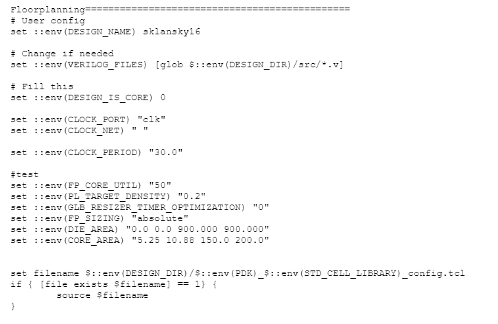
Run floorplan on OpenLane:
# User config
set ::env(DESIGN_NAME) ksa16

# Change if needed
set ::env(VERILOG_FILES) [glob $::env(DESIGN_DIR)/src/*.v]

# Fill this
set ::env(DESIGN_IS_CORE) 0

set ::env(CLOCK_PORT) "clk"
set ::env(CLOCK_NET) " "

set ::env(CLOCK_PERIOD) "30.0"


#test
set ::env(FP_CORE_UTIL) "80"

set ::env(FP_SIZING) "absolute"
set ::env(DIE_AREA) "0.0 0.0 1000.000 1000.000"
set ::env(CORE_AREA) "5.25 10.88 900.0 900.00"

set filename $::env(DESIGN_DIR)/$::env(PDK)_$::env(STD_CELL_LIBRARY)_config.tcl
if { [file exists $filename] == 1} {
	source $filename
}
magic -T /home/ProgramFiles/openlane/pdks/sky130A/libs.tech/magic/sky130A.tech lef read ../../tmp/merged.lef read Sklansky16.floorplan.def
file:///home/ut01/Documents/FINAL/OPENLANE/SKLANSKY16/SKLANSKY/SKLANSKY_floor%20plan.png
- Bind the netlist to a physical cell with real dimensions. The physical cell will come from a library that can provide multiple options for shapes, dimensions, and delay for same cells.
- Next is placement of those physical cells to the floorplan.
- Optimize placement to maintain signal integrity. This is where we estimate wirelength and capacitance (C=EA/d) and based on that insert repeaters/buffers. The wirelength will form a resistanace which will cause unnecessary voltage drop and a capacitance which will cause a slew rate that might not be permissible for fast current switching of logic gates. The solution to reduce resistance and capacitance is to insert buffers for long routes that will act as intermediary and separate a single long wire to multilple ones. Sometime we also do abutment where logic cells are placed very close to each other (almost zero delay) if it has to run at high frequency (2GHz). Crisscrossing of routes is a normal condition for PnR since we can use separate metal layer (using vias) for crisscrossed path.
- After placement optimization, We will setup timing analysis using idle clock (zero delay for wires and has no clock buffer related delays) considering we have not yet done CTS.
The goal of placement is not yet on timing but on congestion. Also, standard cells are not placed on floorplan stage, it is done on Placement stage. Macros or preplaced cells are the ones placed on floorplan stage.Macros or preplaced cells are placed on floorplan stage.
Placement: % run_placement. This commmand is a wrapper which does global placement (performed by RePlace tool), Optimization (by Resier tool), and detailed placement (by OpenDP tool). It displays hundreds of iterations displaying HPWL and OVFL. The algorithm is said to be converging if the overflow is decreasing. It also checks the legality.
magic -T //home/ProgramFiles/openlane/pdks/sky130A/libs.tech/magic/sky130A.tech lef read ../../tmp/merged.lef read Sklansky16.placement.def
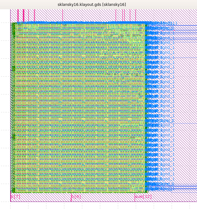
file:///home/ut01/Documents/FINAL/OPENLANE/SKLANSKY16/SKLANSKY/SKLANSKY16_placement.png
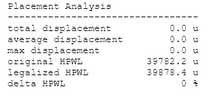
Placement Analysis
---------------------------------
total displacement          0.0 u
average displacement        0.0 u
max displacement            0.0 u
original HPWL           38587.4 u
legalized HPWL          38757.8 u
delta HPWL                    0 %
Placement is done on two stages:
- Global Placement = placement with no legalizations and goal is to reduce wirelength. It uses Half Perimeter Wirelength (HPWL) reduction model.
- Detailed Placement = placement with legalization where the standard cells are placed on stadard rows, abutted, and must have no overlaps
After extracting the modified verilog netlist after doing timing ECO, run_floorplan and run_placement and then run_cts. In CTS, the verilog netlist is modified to add the clock buffers and this new verilog netlist is saved under /runs/[date]/results/cts/.
run_cts and the other OpenLane commands are actually just calling the tcl proc (procedure) inside /OpenLane/scripts/tcl_commands/. This tcl procedure will then call OpenROAD to run the actual tool. For example, run_cts can be found inside /OpenLane/scripts/tcl_commands/cts.tcl, this tcl procedure will call OpenROAD and will call /OpenLane/scripts/openroad/cts.tcl which contains the OpenROAD commands to run TritonCTS.
Inside the /OpenLane/scripts/openroad/cts.tcl contains the configuration variables for CTS. Notables ones are:
CTS_CLK_BUFFER_LIST= list of clock branch buffers (sky130_fd_sc_hd__clkbuf_8sky130_fd_sc_hd__clkbuf_4sky130_fd_sc_hd__clkbuf_2)CTS_ROOT_BUFFER= clock buffer used for the root of the clock tree and is the biggest clock buffer to drive the clock tree of the whole chip (sky130_fd_sc_hd__clkbuf_16)CTS_MAX_CAP= maximum capacitance of the output port of the root clock buffer.
One simple routing algorithm is Maze Routing or Lee's routing:
- The shortest path is one that follows a steady increment of one (1-to-9 on the example below). There might be multiple path like this but the best path that the tool will choose is one with less bends. The route should not be diagonal and must not overlap an obstruction such as macros.
- This algorithm however has high run time and consume a lot of memory thus more optimized routing algorithm is preferred (but the principles stays the same where route with shortest path and less bends is preferred)
DRC Cleaning: DRC cleaning is the next step after routing. DRC cleaning is done to ensure the routes can be fabricated and printed in silicon faithfully. Most DRC is due to the constraints of the photolitographic machine for chip fabrication where the wavelength of light used is limited. There are thousands of DRC and some DRC are:
- Minimum wire width
- Minimum wire pitch (center to center spacing)
- Minimum wire spacing (edge to edge spacing)
- Signal short = this can be solved my moving the route to next layer using vias. This results in more DRC (Via width, Via Spacing, etc.). Higher metal layer must be wider than lower metal layer and this is another DRC.

OpenLane routing stage consists of two stages:
- Global Routing - Form routing guides that can route all the nets. The tool used is FastRoute
- Detailed Routing - Uses the global routing's guide to actually connect the pins with least amount of wire and bends. The tool used is TritonRoute.
Triton Route
- Performs detailed routing and honors the pre-processed route guides (made by global route) and uses MILP based (Mixed Integer Linear Programming algorithm) panel routing scheme(uses panel as the grid guide for routing) with intra-layer parallel routing (routing happens simultaneously in a single layer) and inter-layer sequential layer (routing starts from bottom metal layer to top metal layer sequentially and not simultaneously).
- Honors preferred direction of a layer. Metal layer direction is alternating (metal layer direction is specified in the LEF file e.g. met1 Horizontal, met2 Vertical, etc.) to reduce overlapping wires between layer and reduce potential capacitance which can degrade the signal.

Command used : run_routing
Routing resources analysis :
Routing resources analysis :===============================
[INFO GRT-0053] Routing resources analysis:
          Routing      Original      Derated      Resource
Layer     Direction    Resources     Resources    Reduction (%)
---------------------------------------------------------------
li1        Vertical       311040          4004          98.71%
met1       Horizontal     414720        370761          10.60%
met2       Vertical       311040        310596          0.14%
met3       Horizontal     207360        207064          0.14%
met4       Vertical       124416        123148          1.02%
met5       Horizontal      41472         41184          0.69%
---------------------------------------------------------------
Final Congestion report :
[INFO GRT-0096] Final congestion report:
Layer         Resource        Demand        Usage (%)    Max H / Max V / Total Overflow
---------------------------------------------------------------------------------------
li1               4004             0            0.00%             0 /  0 /  0
met1            370761          2585            0.70%             0 /  0 /  0
met2            310596          2959            0.95%             0 /  0 /  0
met3            207064             0            0.00%             0 /  0 /  0
met4            123148             0            0.00%             0 /  0 /  0
met5             41184             0            0.00%             0 /  0 /  0
---------------------------------------------------------------------------------------
Total          1056757          5544            0.52%             0 /  0 /  0
Best reference for this the Triton Route paper.
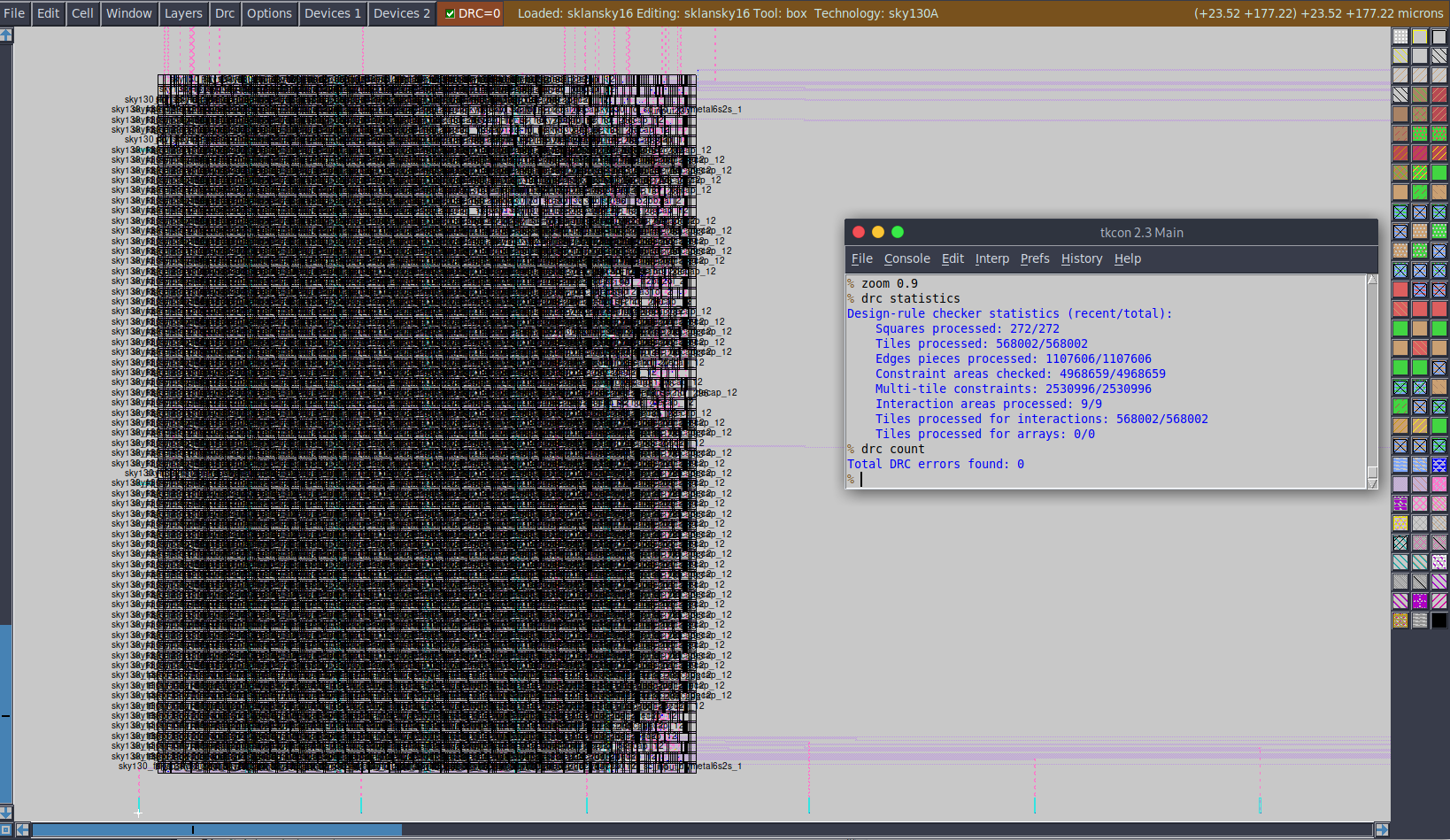
magic -T /home/ProgramFiles/openlane/designs/Sklansky16/runs/SKLANSKY16/results/magic/Sklansky16.mag
Library Characterization: Of all RTL-to-GDSII stages, one common thing that the EDA tool always need is data from the library of gates which keeps all standards cells (and, or, buffer gates,...), macros, IPs, decaps, etc. Same cells might have different flavors inside the library (different sizes, delays, threshold voltage). Bigger cell sizes means bigger drive strength to drive longer and thicker wires. Bigger threshold voltage (due to bigger size) will take more time to switch(slower clock) than those with smaller threshold voltage.
A single cell needs to go through the cell design flow. The inputs to make a single cell comes from the foundry Process Design Kits:
- DRC & LVS Rules = tech files and poly subtrate paramters (CUSTOME LAYOUT COURSE)
- SPICE Models = Threshold, linear regions, saturation region equations with added foundry parameters. Including NMOS and PMOS parameteres (Ciruit Deisgn and Spice simulation Course)
- User defined Spec = Cell height (separation between power and ground rail), Cell width (depends on drive strength), supply voltage, metal layer requirement (which metal layer the cell needs to work)
The library cell developer must adhere to the rules given on the inputs so that when the cell is used on a real design, there will be no errors. Next is design the library cell:
- Design the circuit function (Output: circuit design language (CDL))
- Model the pmos and nmos that meets input library requirement
- Layout the design using Euler's path and sticky diagram to produce best area. This can be done on
magiclayout tool.The outputs are:- GDSII (layout file)
- LEF (defines the width and height of cell)
- extract spice netlist .cir (parasitics of each element of cell: resistance, capacitance) After design is characterization using GUNA software, where the outputs are timing, noise, and power characterization.
Here is a great video guide on layout using Magic. And here is the Magic website with tutorials.
- Left click = lower-left corner of box
- Right click = upper-right corner of box
- "z" = zoom in, "Z" = zoom out, "ctrl + z" = zoom into the box
- Middle click on empty area will turn the box into empty (similar to erasing it)
- "s" three times will select all geometries electrically connected to each other
:box= display parameters of selected box:grid0.5um 0.5um = turn on/off and set grid:snap user= snap based on current grid:help snap= display help for command:drc style drc(full)= use all DRC when doing DRC checking:paint poly= paint "poly" to current box:drc why= show drc violation inside selected area (white dots are DRC violations ):erase poly= delete poly inside the box:select area= select all geometries inside the box:copy n 30= copy selected geometries to North by 30 grid steps:move n 1= move selected geometries to North by 1 step ("." to move more, "u" to undo): select cell _08555_= select a particular cell instance (e.g. cell _08555_ which can be searched in the DEF file):cellname allcells= list all cells in the layout:cellname exists sky130_fd_sc_hd__xor3_4= check if a cell exists:drc why= show DRC violation and also the DRC name which can be referenced from Sky130 PDK Periphery Rules.
Open the def file via magic with no DRC errors:
magic -T /home/ProgramFiles/openlane/designs/Sklansky16/runs/SKLANSKY16/results/magic/Sklansky16.gds
...........
DESIGN ksa16 ;
UNITS DISTANCE MICRONS 1000 ;
DIEAREA ( 0 0 ) ( 1000 1000 ) ;
............
The die area here is in database units and 1 micron is equivalent to 1000 database units. ** Thus area of the die is (1000/1000)microns*(1000/1000)microns = 1 microns squared.**
/home/ProgramFiles/caravel_user_project/openlane/user_proj_example/runs/user_proj_example/reports/manufacturability_report.rpt
Design Name: user_proj_example
Run Directory: /project/openlane/user_proj_example/runs/user_proj_example
----------------------------------------

Magic DRC Summary:
Source: /project/openlane/user_proj_example/runs/user_proj_example/reports/magic/38-magic.drc
Total Magic DRC violations is 0
----------------------------------------

LVS Summary:
Source: /project/openlane/user_proj_example/runs/user_proj_example/results/lvs/user_proj_example.lvs_parsed.lef.log
LVS reports no net, device, pin, or property mismatches.
Total errors = 0
----------------------------------------

Antenna Summary:
Source: /project/openlane/user_proj_example/runs/user_proj_example/reports/routing/40-antenna.rpt
Number of pins violated: 0
Number of nets violated: 0
With this Report we place an SoC, So we need to do in Carvel Harness
/home/ProgramFiles/openlane/designs/Sklansky16/runs/final/reports/manufacturability_report.rpt
Design Name: ksa16
Run Directory: /openLANE_flow/designs/ksa16/runs/KSA16
----------------------------------------

Magic DRC Summary:
Source: /openLANE_flow/designs/ksa16/runs/KSA16/reports/magic/47-magic.drc
Total Magic DRC violations is 0
----------------------------------------

LVS Summary:
Source: /openLANE_flow/designs/ksa16/runs/KSA16/results/lvs/ksa16.lvs_parsed.lef.log
LVS reports no net, device, pin, or property mismatches.
Total errors = 0
----------------------------------------

Antenna Summary:
Source: /openLANE_flow/designs/ksa16/runs/KSA16/reports/routing/49-antenna.rpt
Number of pins violated: 0
Number of nets violated: 0
![]()
![]()
| ❗ Important Note |
|---|
Refer to README for a quickstart of how to use caravel_user_project
Refer to README for this sample project documentation.