I. Introduction
Recently complexity has been shifting from hardware to software. 32-bit CPU cores themselves are becoming a commodity. To create anything useful, applications require complex software stacks. Traditional microcontroller chip vendors had their own compilers, IDE tools, software vocabulary and libraries. This lock-in approach works for small software but does not scale for IoT where network and security code are involved. For this reason, modern software developers require commodity tools like GCC and Clang rather than closed proprietary development tools. Microcontroller vendors need to join and actively participate in collaborative open source projects, which major players like Apple, Intel, ARM and recently also RISC-V have been doing.
One unique aspect of the SH architecture is that the ISA intellectual property ownership belongs to the public and its ability to run Linux with MMU and without MMU. Running Linux exposes the whole system to a lot of various use and test cases, which is difficult to achieve otherwise. At the same time, SH cores can be implemented in a compact and energy efficient manner. In general, 2-stage pipeline implementation achieves higher cycle performance than that of 5-stage pipeline for the same architecture. However, SH software support has been left behind recently, there are some deficits w.r.t. automatic compiler optimizations, which are crucial for modern software. Therefore, we will make the software support up to date, and show the latest evaluation result when we apply the presentation slides.
II. 2-Stage Pipeline SH-2 CPU
In 2015 we started designing the 2-stage pipeline SH-2 CPU in a clean room. We wrote the RTL of the CPU in System Verilog, used Perl script to assemble the micro-sequence description to System Verilog, simulated the RTL with Modelsim, and synthesized the RTL to Intel Max 10 FPGA device. Our design runs at 50MHz clock speed on the FPGA device. We believe the 2-stage-pipeline design is advantageous because (1) the branch instruction is faster due to shallow pipeline, (2) lower number of logic elements are consumed due to fewer pipeline stages, (3) the design achieves faster clock due to the simpler control and data paths, and (4) we could save the design resource due to the simplicity.

The SH-2 system has tightly coupled memories (TCMs), AHB and APB bus, interrupt controller, UART, PWM and ADC (from Max 10 FPGA).

We conducted a sanity check by constructing real world application brushless DC motor control both sensored and sensorless. The SH-2 FPGA board is connected to a commercial inverter board which contains Gate Driver, coil driver MOSFETs and other circuits, and a Tsukasa TG55L 24V motor.
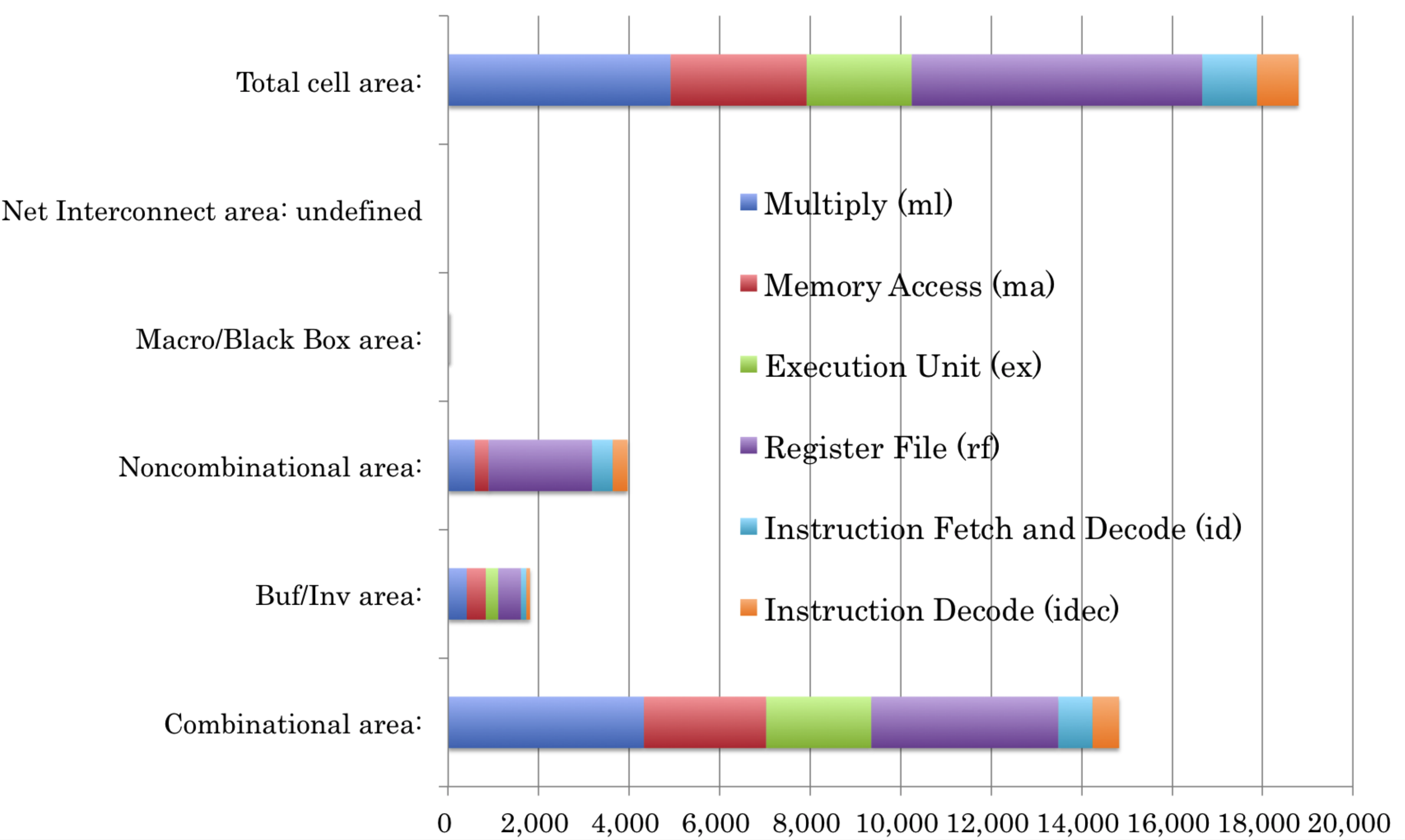
Fig. RISC CPU Area Breakdown: UMC 40nm Low Power Process
III. Implementation Results
Table 1 shows the implementation results of our 2-stage pipeline SH-2 CPU (H27604) on Intel Max 10 FPGA. The table also shows the comparison between our CPU and other similar CPUs. Aquarius is an open source CPU designed by Thorn Aitch and published in OpenCores [6]. Aquarius executes SH-2 instructions with 5-stage pipeline. SCR1 is also an open source CPU designed by Syntacore [8]. SCR1 executes RISC-V instructions with 2 to 4-stage pipeline. In Table 1, there are two versions of SCR1. SCR1(1) implements RV32IC ISA which includes 47 Integer (32bit encoding) instructions and 27 Compact (16bit encoding) instructions. SCR1(2) implements RV32IMC ISA which includes RV32IC + 8 Multiply/Divide instructions. As shown in Table 1, our 2-stage SH-2 CPU is the smallest and consumes only 4,655 logic cells and two 18x18 multipliers, while the clock frequency is comparable to other CPUs.
IV. Performance Evaluation
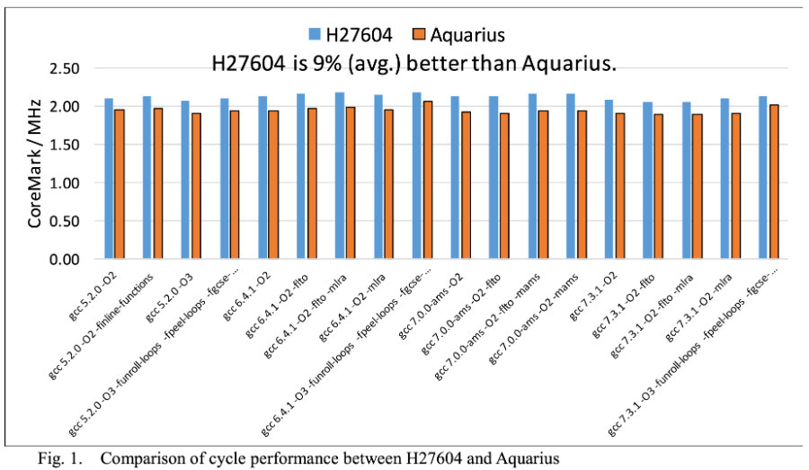
Fig. 1 shows the comparison of cycle performance between H27604 and Aquarius. EEMBC CoreMark [10] and various GCC versions and options were used for the comparison. As shown in Fig. 1, H27604 achieves 9% (avg.) better cycle performance than Aquarius.

V. Conclusion
We developed 2-stage-pipeline SH-2 CPU small and achieves good cycle performance. We implemented the CPU with some peripheral modules on Intel MAX 10 FPGA. The CPU consumes only 4,655 logic cells and can operate at 50MHz. We successfully demonstrate the FPGA system could control the brushless DC motor. The CPU consumes only 33KG of 40nm NVM process at 240MHz, and 20KG of 0.18um process at 80MHz. The CPU can be easily incorporated into FPGA and SoC for IoT, edge AI and robotic applications.
REFERENCE
[1] Hitachi America Ltd., SuperH RISC Engine SH-1/SH-2 Programming Manual, September 3, 1996.
[2] Shumpei Kawasaki et al., “MICROCOMPUTER HAVING 16 BIT FIXED LENGTH INSTRUCTION
FORMAT”, US Patent 5,682,545, Granted Oct 28, 1997.
[3] Motorola, Inc. v. Hitachi, Ltd., US District Court for the Western District of Texas - 750 F. Supp. 1319
(W.D. Tex. 1990) , April 13, 1990, Justia US Law,
https://law.justia.com/cases/federal/district-courts/FSupp/750/1319/1473344/.
[4] The United States Department of Justice, Antitrust Division, UNITED STATES' MEMORANDUM ON THE
1969 CASE, Case: U.S. v. IBM Corp. Date: Thursday, October 5, 1995.
https://www.justice.gov/atr/case-document/united-states-memorandum-1969-case.
[5] The United States Patent and Trademark Office, Introduction,
https://www.uspto.gov/web/offices/pac/mpep/mpep-0020-introduction.html.
[6] Thorn Aitch, “A Pipelined RISC CPU Aquarius (SH-2 ISA Compatible CPU Core) Rev 1.1,” July 21, 2003.
[7] Open Processor Foundation, J-Core, June, 2015 (deplecated).
[8] Syntacore SCR1 Microcontroller Core, https://syntacore.com/page/products/processor-ip/scr1.
[9] Gcc Wiki, Google Summer Of Code 2018 Project, "Implement a (prototype) addressing mode selection
(AMS) pass as a replacement of auto-inc-dec.", https://gcc.gnu.org/wiki/SummerOfCode.
[10] EEMBC CoreMark Benchmark, https://www.eembc.org/coremark/about.php

Our submission to Google sponsored open source shuttle consists of a 2-stage pipeline SH-2 CPU core (H27604). 21 inventors of Hitachi filed SH Instruction Set Architecture (ISA) patent with full ISA behavioral description in C language in 1991. Hitachi and Renesas split this invention into hundred of patents worldwide. A broad right was granted by USPTO on US5682545A. ARM 7TDMI, 9TDMI and MIPS16 used this invention hence ARM is rumored to have paid largest sum of money for IP to acquire its usage rights. These patents expired on October 18, 2014. Thereafter the invention have belonged to the public domain per rules of patents. There have been number of open source SH-2 implementations disclosed in Verilog and VHDL. The earliest such open source SH-2 was "Aquarius" submitted to opencores.org in 2003. The 5-stage pipeline "Aquarius" might have inspired OpenRISC, a foray into the open source ISA, for which now RISC-V is famous for. The SH27604 compiles into 4,655 logic cells of Intel MAX 10 FPGA fabricated on 55nm embedded NOR flash technology, 33K gates of 40nm NVM process running at 240MHz, and 20K gates of 0.18um process running at 80MHz. The MCU incorporates supports for AHB, APB, UART, PWM, and ADC. We plan to apply this solution to IoT, edge AI and robotic applications. GNU and other compilers, assemblers, simulators, debuggers support the CPU. On November 22, 1994 Sega Saturn was introduced to the market. 20 years later on August 10, 2014, former Hitachi engineers purchased a spot a SH-2 demo desk at Hotchips 26. This desk was next to the RISC-V group. (Keywords: ISA, microarchitecture, IoT, edge AI, robotic application, BLDC motor, FPGA, SoC)
TBD
processor
sky130A