This is the Google/EFabless/Skywater Caravel submission of an Analog Spiking Neuron Circuit. The submission also includes a SONOS transistor array.
The circuit in the original paper is in 130nm technology and has a vdd of 300mV. Skywater pdk is hybrid 180nm/130nm node where the minimum transistor length is 150nm. As a result vdd needs to be higher in order to get the circuit to work properly. In simulation 700mV seems to work well.

| node | pad | node | pad | node | pad | |--------|-------------|-----------|-------------|-------------|-------------| | i_bias | mprj_io[13] | v_buff | mprj_io[22] | vdd | vdda1 | | vad | mprj_io[14] | u_buff | mprj_io[23] | vss | vssa1 | | vr | mprj_io[15] | a_buff | mprj_io[24] | vdd_aux | vdda2 | | vk | mprj_io[16] | axon_buff | mprj_io[25] | | vth | mprj_io[17] | sel | mprj_io[26] | | vw | mprj_io[18] | v_syn | mprj_io[27] | | vau | mprj_io[19] | u_syn | mprj_io[28] | | vsyn0 | mprj_io[20] | a_syn | mprj_io[29] | | vsyn1 | mprj_io[21] | axon_syn | mprj_io[30] | | | | i_in | mprj_io[31] |
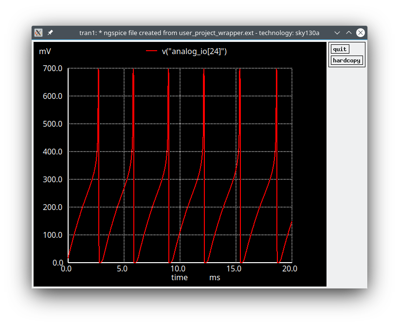
Spiking pattern at v_buff for i_in = 10pA DC
A 2x2 array of nfet sonos cells with transistor sizing 420nmx150nm.

| node | pad | |------|-------------| | WL0 | mprj_io[7] | | WL1 | mprj_io[8] | | BL0 | mprj_io[9] | | SL0 | mprj_io[10] | | BL1 | mprj_io[11] | | SL1 | mprj_io[12] |
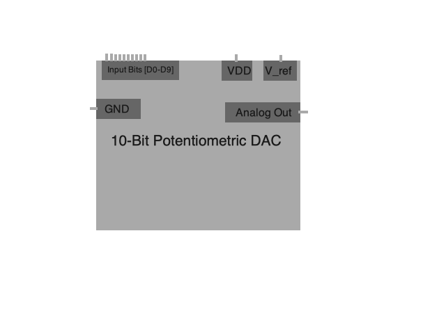
The mega project area also contains a 10-bit Potentiometric Digital to Analog Converter built off of Ashutosh Sharma's design. The design uses a 3.3V rail voltage, and 1.8V digital input voltage. The DAC's inputs are controlled by the Caravel harness' built in RISC-V core. Ashutosh Sharma's design used the OSU180 process, for the caravel submission it was ported to the Sky130 process.
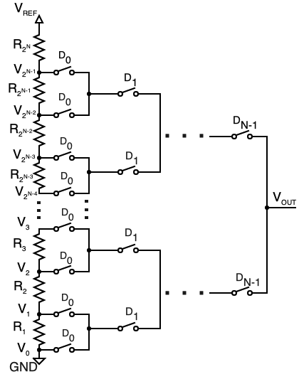
The design uses a string of polysilicon resistors in series to create a string DAC. The resistors are connected to digital switches in order to achieve an exact voltage at the output. The device was built through hierarchical sub-circuits and sub-layouts starting off at 2-bit, then 3-bit and so forth, incrementally reaching 10-bit. With a full scale of 3.3 V and a 10 bit resolution.
| Node | Pad | | :------------ | ------------- | | Analog_Out | analog_io[25] | | Digital_In[0] | io_in[0] | | Digital_In[1] | io_in[1] | | Digital_In[2] | io_in[2] | | Digital_In[3] | io_in[3] | | Digital_In[4] | io_in[4] | | Digital_In[5] | io_in[5] | | Digital_In[6] | io_in[6] | | Digital_In[7] | io_in[7] | | Digital_In[8] | io_in[8] | | Digital_In[9] | io_in[9] | | VDD | vdda1 | | Gnd | vssa1 |
String of resistors and switches that make up potentiometric DAC.
Simple block representing all inputs and outputs of DAC.
To setup and install the repo for development:
```shell export PDK_ROOT=(where pdks will be installed)
cd \$PDK_ROOT
git clone https://github.com/efabless/openlane.git -b mpw-one-a
cd openlane export OPENLANE_ROOT=\$(pwd) make ```
2. Clone and uncompress the repo:
shell
git clone https://github.com/Bryce-Readyhough/caravel_UNCC_MPW_1.git
make uncompress -j\$nproc

A 10 bit DAC and an analog neural network neuron.
1.00
Test Harness
sky130A