5G is an emerging communication technology, which promises higher data rates and lower latency. 5G technology utilizes MIMO architectures to optimize beamforming and reduce interference. MIMO architectures consist of multiple transmitter and receiver chains as shown in Figure 1. For on-chip cost effective solutions, power and area of individual RF components must be optimized. One such component is low noise amplifier (LNA) of receiver. LNA is a critical component because it dictates the noise figure of the entire receiver chain. Lower noise figure means higher receiver sensitivity. For MIMO systems, a low noise amplifier should have following specifications:

LNA utilizes on-chip inductors for gain peaking and input matching. However, inductors occupy large silicon area. An inductor-less LNA design saves huge area and enables wide band operation since no sharp resonance is present. Noise figure can be reduced by feedback and feed forward techniques. The schematic of the proposed inductor less LNA is shown in Figure 2. This design is inspired from this ISSCC paper [1].
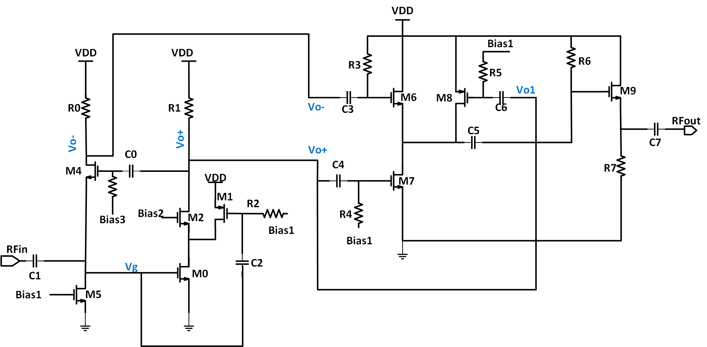
This design has several features. It achieves wide band input match using transistor M4. The size of M4 required for matching is also reduced due to feedback. The gain of circuit is increased by current reuse (M1) and cascode technique (M2). Partial thermal noise of transistors M0, M1 and M2 is cancelled using the feedback. In [1], the noise contribution of M4 is not cancelled. In the proposed design, the noise figure of M4 is also cancelled using feed forward noise cancellation technique (M6-M7). Usually, feedforward technique introduces additional noise figure due to the parallel feed forward path [2]. However due to the inherent parallel path, no extra noise at input is introduced. Also, the voltage at Vo- gives extra gain without any power consumption as compared to [1]. The proposed modifications can result in decreased noise figure and increased voltage gain in the same area and power. The target specifications of the proposed design are summarized in Table 1.
Table 1 Target Specifications
|
Specification |
Target |
|
Bandwidth |
1-5 GHz |
|
Noise Figure |
~3 dB |
|
Power |
<20mW |
|
S11 |
<-10 dB in Band |
|
Voltage Gain |
>=20 dB |
|
1 dB Compression |
>=-20 dBm |
|
Area |
~0.04 sq mm |
Schematic, Layout, GDS, Measurement Results, Design Report
|
[1] |
R. Ramzan, "A 1.4V 25mW Inductor less Wideband LNA in 0.13μm CMOS," in ISSCC, 2007. |
|
[2] |
B. Razavi, RF Microelectronics (Chapter 5), 2nd ed., Prentice Hall. |
This is a proposal for IEEE PICO design contest. An inductor less 5G Bi-Directional amplifier design is proposed that provides wide band operation with low power, area, and noise figure. The design is an improvement on a low noise amplifier design published in ISSCC.
opamp