Description
Most of the present day CMOS ICs require multiple on chip temperature sensors and are applied in varied fields like microprocessors and SOCs, IoT processors and biomedical and health care applications. These temperature sensors are generally distributed in SoC’s to monitor temperatures and their gradients at various locations and give digital read outs. In the case of complex ICs, these readouts are then used in elaborate calibration cycles. Also, in many emerging applications, one must also have fast temperature conversion rates to enable control actions based on certain read out values to be almost instantaneous. Since these sensors are auxillary circuits, power consumed by these sensors must be very low. Further, these temperature sensors should occupy minimal area so that it can be distributed in power sensitive domains of an SoC. Recently a large volume of research articles has emerged reporting different circuit alternatives and realizations in this domain.
Motivated by these developments, the present work targets to design a complete CMOS based temperature sensor unit. The present project will use a resistor based temperature sensor embedded in a Wein Bridge (WB) filter which is incorporated as a subblock in a Frequency Lock Loop (FLL). The resulting frequency of the FLL under locked condition will contain information regarding temperature variations of the sensor. The loop parameters of FLL and circuit blocks in the FLL will be designed carefully such that the circuit noise contribution is minimized. The frequency information will be recorded digitally by using a counter based read out circuit. The other major issue that will be addressed is the calibration of the nonlinear resistance of the temperature sensor spread over the desired temperature range by means of single point trimming.
Design Goals
A compact temperature sensor using polysilicon based thermistor for -35oC to +125oC as proposed by Jan A. Angevare and Kofi A. Makinwa is shown to meet the state of art requirements. This present work will focus in the same direction, and proposes to realize a temperature sensor and its read out circuit meeting minimized jitter, fast settling and power over a wide temperature range. The loop parameters of FLL and all its functional subblocks will be chosen such that a minimal jitter performance is attained and the read out resolution and convergence rate of the sensor is expected to be optimal for the entire range of temperature.
Specification of the system to be realized are as follows:
Temperature range and accuracy : -35oC to +125oC ,
Nominal values of polysilicon resistors and its fringe capacitor of WB : 135kΩ and 5pF
Read out counter : 20 bit
RTC clock : 32 kHz derived from 131kHz crystal to drive counter
WB nominal input frequency : 250kHz
VCO nominal frequency : 1MHz
Process used : 0.13µm SKY130A process
Outcome of this project will be as follows:
Block Diagram
The present project realizes temperature sensor using thermistor in an RC based Wein Bridge (WB) filter. The WB filter realized, is a band pass filter which under bridge balance condition, the transfer function’s phase response is zero at the WB filter centre frequency and varies linear as a function of frequency deviation for very small frequency deviations.
As resistance varies with temperature, bridge becomes unbalanced, leading to phase shift from its nominal value. This phase shift is detected in a negative feedback FLL shown in the functional block diagram given in Fig.1 and corrected by adjusting the frequency of the excitation signal. Thus the temperature variation is embedded in the excitation frequency which is read out in digital format by the frequency to digital converter.

FLL block in the system comprises of WB filter, mixer, Voltage Controlled Oscillator (VCO) and divider. Output of VCO will act as excitation signal with RMS voltage Vdrive. The response from the filter will be mixed with VCO output in mixer which in turn acts a phase detector. From the output of mixer, an average error voltage will be derived by the capacitor Cint, in proportion to the phase error from the filter. This error voltage acts as control voltage for VCO, controlling its frequency in the loop such that phase error is reduced to zero. Under locked condition, the VCO frequency will contain information about the temperature. The frequency information is digitally coded by counting the zero crossings of FLL output signal.
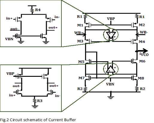
Schematics
The circuit architecture that will be chosen for mixer will be a chopped current buffer (CB) architecture based on [1] and its circuit schematic is shown in Fig.2. Chopping in current buffer serves two purposes namely, phase detection by the process of mixing and up conversion of flicker noise. The average voltage resulting from phase detection will be verified for various resistance values inturn for various temperature values. Serving as a chopper, the flicker noise will be upconverted and its contribution will become less significant.
A ring oscillator based topology will be chosen for VCO architecture that has to serve as an ideal reference with supply and process parameter independent features. The prelimnary design will be carried using current starved single ended ring oscillator as realized in [1]. In the subsequent cycles of realization, the delay cell of the oscillator shall be designed for minimum jitter contribution and supply sensitivity.
Presently, preliminary work on design and functional verification of all the circuit blocks of FLL as well as integration has been carried out using Cadence Spectre simulation tool using 0.18µm CMOS process library. Noise performance analysis of the circuit functional blocks has also been carried out. Noise performance of Current buffer with chopper incorporated is shown in Fig.3.

The VCO gain characteristic of a nine stage current starved single ended inverter with Cascode load is shown in Fig.4. VCO gain characteristic is observed to be 4.83 MHz/V sensitivity with linear range defined from 240 kHz to 1.8 MHz.

In the present work, these functional blocks will be transformed to 0.13µm SKY130A process and a complete integration will be carried out to realize the temperature sensor meeting the targeted specification.
References
1] Pyoungwon Park, David Ruffieux, Kofi A.A. Makinwa, ‘’A Thermistor-Based Temperature Sensor for a Real-Time Clock With 2ppm Frequency Stability’’, IEEE Journal of Solid-State Circuits, Vol.50, No.7,Jul. 2015, pp 1571- 1580.
2] Sining Pan, Yanquan Luo, Saleh Heidary Shalmany, and Kofi A. A. Makinwa, ‘’A Resistor-Based Temperature Sensor With a 0.13 pJ·K2 Resolution FoM’’ IEEE Journal of Solid-State Circuits, Vol.53, No.1 ,Jan. 2018, pp 164- 173.
3] Woojun Choi1, Yong-Tae Lee, Seonhong Kim, Sanghoon Lee, Jieun Jang, Junhyun Chun, Kofi A. A. Makinwa, Youngcheol Chae1A “0.53pJ∙K2 7000μm2 Resistor-Based Temperature Sensor with an Inaccuracy of ±0.35°C (3σ) in 65nm CMOS” IEEE Solid State Circuits Conference, 2018.
Team members
Project Coordinator : Dr. J Dhurga Devi
The other participating members are
Polysilicon resistor based temperature sensor and its read out electronics
sensor