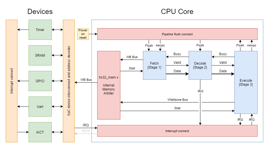
The HSC Latte HS32 Core is a 32-bits RISC CPU. The HS32 Core has 32-bits instructions and 16 32-bits registers.
Below is a list of HS32 Core Project Directories:
| Repository | Description | License | Issues | Stars | Contributors |
| ----------------------------------------------------------------- | ----------------------- | ---------------------------------------------------------------------------- | -------------------------------------------------------------------------- | ------------------------------------------------------------------------ | -------------------------------------------------------------------------------------- |
| caravel-hs32core | Core Harness | 


HS32 is a RISC-type CPU. (...)
| Path | Description |
|-|-|
| verilog/rtl/hs32cpu | CPU Core Submodule |
| verilog/rtl/hs32_user_proj | User project files and wrapper |
| verilog/rtl/hs32cpu/docs | Detailed core documentation |
| verilog/dv/hs32_nocaravel | No-caravel testbenches |
| verilog/dv/caravel/hs32_soc | Caravel-integrated testbenches |
These are the different encodings that instructions come in.
All instructions are 32 bit.
The first 8 bits is opcode.
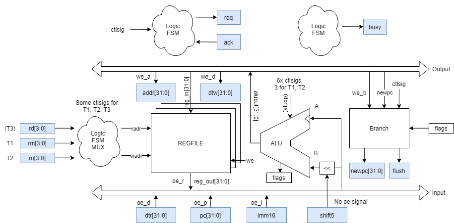
Rd, Rm, Rn are always in the same position in the instruciton if present
| A | B | C | D | E | F | G | H | I | |
|---|---|---|---|---|---|---|---|---|---|
|
1
|
Name | [0:3] | [4:7] | [8:11] | [12:15] | [16:19] | [20:23] | [24:27] | [28:31] |
|
2
|
I-Type (Immediate) |
Opcode | Rd | Rm | Imm16 | ||||
|
5
|
R-Type (Register) |
Opcode | Rd | Rm | Rn | Shift | Shift | Shift Direction | Register Bank | Register Bank | XXX | |
There are 16 (r0-r15) general-purpose registers plus 4 privileged registers. In supervisor mode, r12-15 is separate from user-mode r12-15. In all modes, r14 and r15 will be used as the link register and stack pointer respectively.
Legend:
| Register | Alias/Description | ||
| User | IRQ | Supervisor | |
| r0-r11 | |||
| r12 | General | ||
| r13 | General | ||
| r14 | User LR | IRQ LR | Super LR |
| r15 | User SP | IRQ SP | Super SP |
During a mode switch, the return address will be stored in the appropriate LR and the return stack pointer will be stored in the appropriate SP.
For instance, an interrupt call from User mode will prompt a switch to IRQ mode. The return address and stack pointer of the caller will be stored in IRQ LR (r14) and IRQ SP (r15) respectively.
WIP

Various timing diagrams of the address and data buses
Clock Cycles: 4 minimum
Timing Requirements:
- The duration of the TW read clock (no data input) is determined by the tpd of whichever memory chip used.
- TW can span multiple clock periods to allow for different memory timings. This will allow the CPU to be clocked at a higher speed than the memory chips.
In the implementation, OE# is the AND of 2 signals, one leading edge and one falling edge-driven signals.

Clock Cycles: 4 minimum
Timing Requirements: - See the read cycle specifications

Apache 2.0 LICENSE
HS32 Core - A 32-bits RISC Processor
``` Copyright (c) 2020 The HSC Core Authors
Licensed under the Apache License, Version 2.0 (the "License"); you may not use this file except in compliance with the License. You may obtain a copy of the License at
https://www.apache.org/licenses/LICENSE-2.0
Unless required by applicable law or agreed to in writing, software distributed under the License is distributed on an "AS IS" BASIS, WITHOUT WARRANTIES OR CONDITIONS OF ANY KIND, either express or implied. See the License for the specific language governing permissions and limitations under the License. ```

Open Source Hardware Processor
1.00
CPU
sky130A