This is a proposal for IEEE PICO design contest. A novel bandgap voltage reference with accurate curvature correction technique is proposed that target sub-ppm temperature coefficient for the wide range of temperature. In addition, the proposed design provides good line regulation and high-power supply rejection ratio. The design is an improvement of state-of-the-art bandgap voltage reference design published in ISCAS.
A number of integrated circuit modules like low-dropout (LDO) regulator, analog-to-digital converters (ADC), DC-DC converters, and power management units (PMU) require highly stable voltage references. The figure of merit of these circuits hugely depends on the accuracy and stability of voltage reference. These circuit are deployed in different environmental conditions, where they are exposed to a wide range of temperatures. For such circuits, if the reference voltage changes with temperature or with any other variation, the performance of these circuits degrade. One application of voltage reference is modern communication system on chip as shown in Fig. 1. The performance of such data acquisition section strongly depends on stability of voltage reference, variation in reference will disturb the performance of the whole system. Bandgap reference (BGR) is electronic circuit that provides stable constant voltage which is independent of temperature, supply voltage and process variation.

Fig 1: Modern communications system on chip
A first order conventional BGR is the summation of base to emitter (VBE) voltage of BJT transistor, which has complementary dependence on absolute temperature, or “CTAT”, with thermal voltage (VT), which has a direct dependence on absolute temperature (“PTAT”). VT temperature coefficient (TC) is constant, resulting in linear temperature response. However, TC of BJT VBE depends on temperature itself, resulting in no-linear temperature response of VBE. Thus, for the first order BGR, the compensation is not effective over wider temperature range. Hence, the first order BGR output exhibits a curvature in reference voltage as shown in Fig. 2.

Fig 2: Curvature in the temperature dependence of a BGR voltage
Other important parameters are power supply rejection ratio (PSRR), line regulation, power consumption, start-up, area, and reference voltage value The proposed design provides curvature correction to reduce the TC, improvement in PSRR, and auto start-up feature to ensure BGR operation during supply voltage transient.
In this proposed solution we will extract silicon bandgap voltage at zero kelvin (VG0), from BJT VBE(T) as shown in equation (1) [1].
![]()
To get temperature independent constant VG0 temperature dependent 2nd and 3rd term of equation (1) should be compensated. 2nd term of equation (1) is CTAT, which will be compensated by adding PTAT term. For the compensation of non-linear 3rd term, three diode connected model shown in Fig. 3 with and self-bootstrapping is opted.

Fig. 3: Three BJT connected as diodes to extract the VGO.
In proposed model, the difference between V1 and V2 generates PTAT term (VPTAT), while the difference between V2 and V3 generates non-linear term (VNL) which have opposite behaviour to the non-linear term in equation (1). Thus, temperature independent VG0 can be achieved, by proper weighted addition of VBE, VPTAT, and VNL as shown in Fig. 4.

Fig. 4: Weighted summation to extract the VG0.
Schematic of the proposed architecture is shown in Fig. 5. Drain terminal of M5 provides uncompensated bandgap reference voltage, which is labelled as labeled as Vo in Fig.5. VPTAT is generated at emitter of Q2, labelled V2. VNL is generated at the emitter terminal of Q3, labelled as V3. Curvature compensated BGR voltage (Vref) is generated by adding Vo, V1, and V2, which compensates the temperature dependent terms, and results in temperature independent VG0. The target performance parameters summary of the proposed design is shown in Table 1.
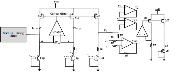
Fig: 5 VGO extractor based on conventional BGR circuit
|
Performance Parameter |
Target |
|
Temperature coefficient (TC) |
<10 ppm/oC |
|
PSRR |
> -50 dB |
|
Line regulation |
< 10 mV/V |
|
Temperature range |
-40 to 125 oC |
Team Leader:
Team Members:
[1] Z. Liu and D. Chen, “A voltage reference generator targeted at extracting the silicon bandgap Vgo from Vbe,” Proc. - IEEE Int. Symp. Circuits Syst., Sep. 2017, doi: 10.1109/ISCAS.2017.8050750.
[2] N. Liu, R. Geiger, and D. Chen, “Bandgap voltage VGO extraction with two-temperature trimming for designing sub-ppm/°C voltage references,” Proc. - IEEE Int. Symp. Circuits Syst., vol. 2019-May, 2019, doi: 10.1109/ISCAS.2019.8702697.
This is a proposal for IEEE PICO design contest. A novel bandgap voltage reference with curvature correction technique is proposed. The proposed design provides less than 10 ppm/oC temperature coefficient for the temperature range of -40oC to 125oC. The proposed design also provides good line regulation and high-power supply rejection ratio, which are less than 10 mV/V, and -50 dB respectively. The design is an improvement of state-of-the-art bandgap voltage reference design published in ISCAS [1] in 2017.
final
bg