Detailed description
Figure 1 shows the Capacitive Transimpedance Amplifier (CTIA) which integrates the photodetector currents and outputs a voltage that represents either the pixel value or the difference between horizontally-adjacent pixels. The switches can control the orientation of the integration capacitor.

Figure 1: Capacitive Transimpedance Amplifier (CTIA)
The RLBP generator (abbreviated as RPG) is shown in figure 2. An input comparator compares the local gradient value for each pixel (Vpixel) to a reference voltage (Vref). When Vpixel > Vref , the digital output of the comparator is 1, and 0 otherwise. The digital comparator outputs are sequentially stored in an array of 3 × 3 flip-flops, organized as three shift registers. The RPG outputs an 8-bit RLBP with the output of all the flip-flops except for the one at the center.

Figure 2: Architecture of the RPG
The digital coprocessor illustrated in figure 3 to perform face recognition. It is composed of four modules, and is responsible for processing the RLPBs of each pixel using LDA projection using LDA coefficients previously calculated, and computing the face classification using euclidean distance. The digital coprocessor outputs the ID of the corresponding subject in the image

Figure 3: Architecture of the digital coprocessor
Figure 4 shows the linear discriminant analysis (LDA) projection module. The module transforms the 8-bit RLBP into a 6-bit uniform RLBP (uRP). For each uRP value received, the module accumulates the value of its corresponding LDA coefficient, thus performing histogram computation and LDA projection in a single step.

Figure 4: Architecture of the LDA projection module

Figure 5: Euclidean distance module
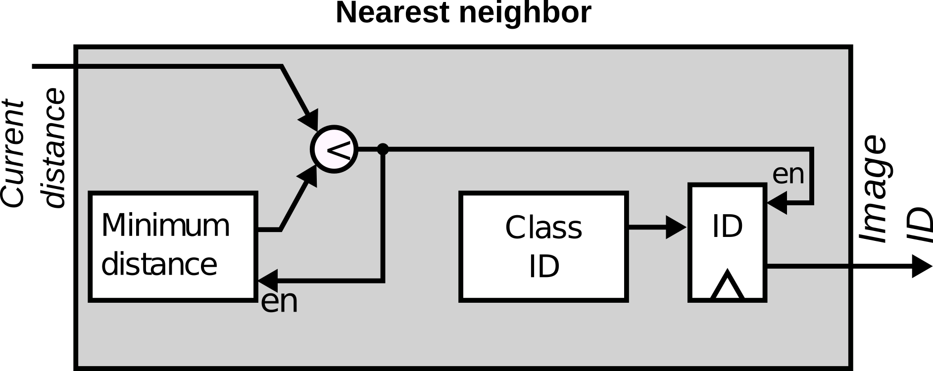
Figure 6: Classification module

Figure 7: Layout of the CTIA and the integration capacitor implemented on the TMSC 0.35 µm process, the schematic can be found in [2].
The FPGA implementation of the digital coprocessor has utilized 4345 LUT, 1298 Flip Flops and two block rams of 4 KB each, however the memory requirements relate to the image and object’s database size. The above mentioned metrics prove that the proposed core can be implemented using the resources of the user project area in the MPW program.
Design Goals
References
[1] Valenzuela, Wladimir, Javier E. Soto, Payman Zarkesh-Ha, and Miguel Figueroa. 2021. "Face Recognition on a Smart Image Sensor Using Local Gradients" Sensors 21, no. 9: 2901. https://doi.org/10.3390/s21092901
[2] Soto, J. E., Valenzuela, W. E., Díaz, S., Saavedra, A., Figueroa, M., Ghasemi, J., & Zarkesh-Ha, P. (2017, December). An intelligent readout integrated circuit (iROIC) with on-chip local gradient operations. In 2017 24th IEEE International Conference on Electronics, Circuits and Systems (ICECS) (pp. 360-362). IEEE. https://doi.org/10.1109/ICECS.2017.8292082
Team Members
Maximiliano Cerda – Team Leader – Student BSc. Eng. University of Bío-Bío, Chile
Darwin Muñoz – Team Member – Student BSc. Eng. University of Bío-Bío, Chile
Mauricio Montanares – Team Member – Student BSc. Eng. University of Bío-Bío, Chile
Norman Mendez – Team Member – Student BSc. Eng. University of Bío-Bío, Chile
Krzysztof Herman – Team Advisor – DSc. Eng. University of Bío-Bío, Chile
Wladimir Valenzuela – Team Advisor – MSc. Eng. University of Concepción, Chile
Jorge Marin - Team Advisor, DSc. Eng. AC3E Canter, Valparaiso, Chile
Abstract: We propose a development of a mixed signal circuit, which processes signals from (CMOS) image sensors in both analog and digital domains in order to perform face recognition. The circuit has three cores: (1) an analog preprocessor, (2) a digital ringed local binary patterns generator (RLBP) and (3) a digital coprocessor, which classifies patterns. The principal advantage of the circuit is that it calculates the local differences between adjacent pixels using analog technique for the whole sensor array simultaneously during the image capture, which significantly reduces the computational effort in the digital domain. Due to the fact that all three stages are scalable, we would like to propose implementation of 3 different versions of the circuits corresponding to the 3x3, 9x9 and 16x16 pixel matrix. The analog part was designed in TSMC 0.35 um process however never tapped-out, but it was tested using post layout parasitics extraction. The digital functionalities and performance were FPGA proven.