IoT devices have become widespread and as such the need for efficient power management has increased. Specifically, battery powered IoT devices in remote deployments (e.g., smart agriculture applications) benefit greatly from efficient power delivery systems that can utilize as much of the stored energy as possible, extending service intervals and reducing maintenance costs. Our design contains a non-PWM novel boost converter topology that can deliver sufficiently high load currents (on the order of tens of mAs) and maintain high output voltage even at low battery levels [1]. We aim to compare their performance characteristics for various load currents and minimum output voltages and examine their peak efficiency as the input voltage drops due to the battery gradual discharge, thus concluding the useful lifetime they allow when leveraged by our converter.
This design is composed of four circuits. A PWM boost converter, two versions of a novel non-PWM boost converter, one including a transformer on the chip and one without (as producing high self-inductance on-chip may be challenging), and a switched-capacitor circuit as shown in the top-level diagram of Fig. 1. These circuits cover a range of battery powered IoT devices’ power demands with current draws in the range of single digit to a couple of tens of milliamperes.

The PWM boost converter, depicted in Fig. 2, contains a PWM block on chip, consisting of a Schmitt trigger and an Integrator that feeds a Comparator. Through its feedback, this implementation can provide satisfying output voltage regulation but with the associated overhead in power incurred by the PWM block. This circuit will serve as the benchmark against which we compare the novel booster topologies.

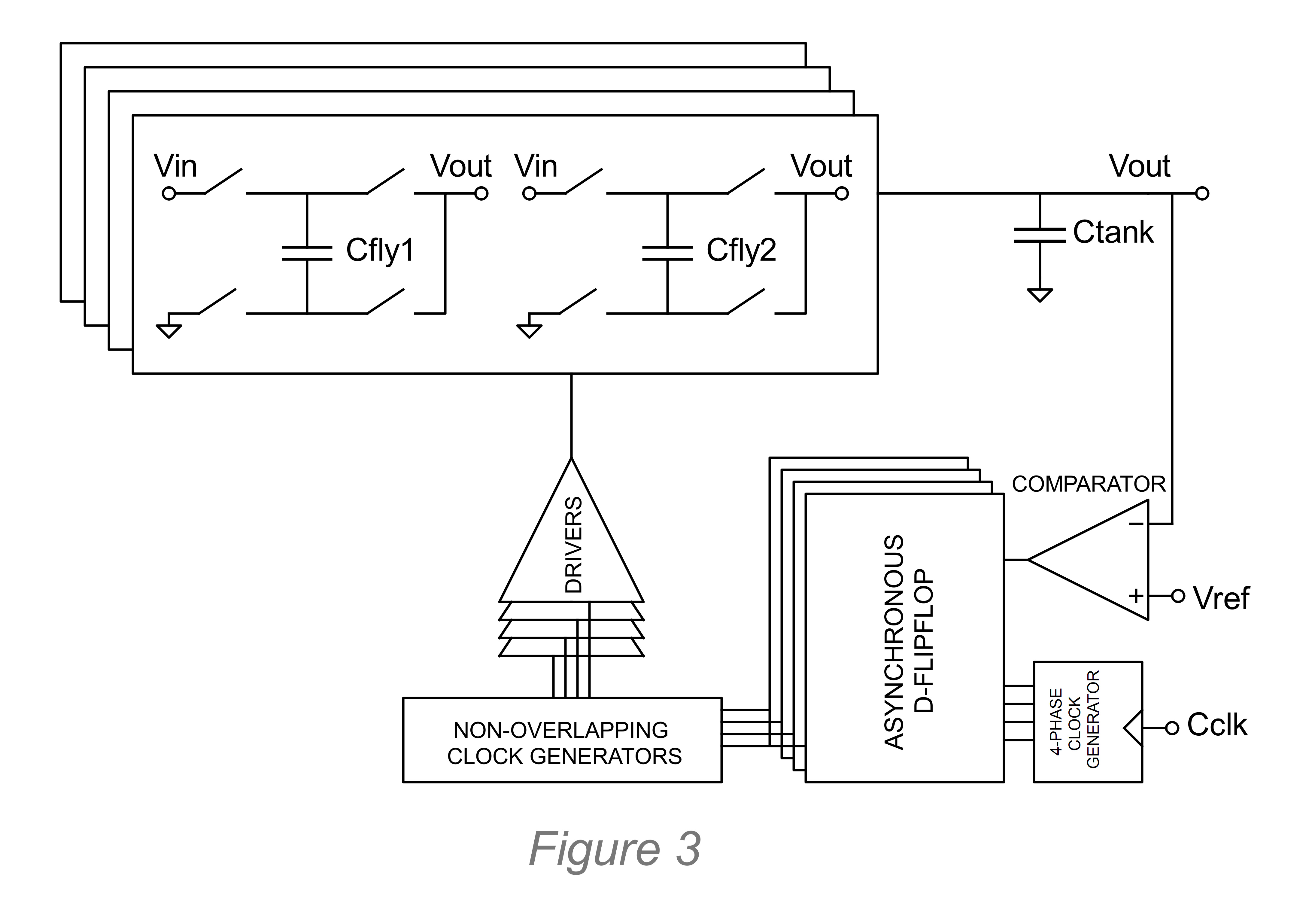
The switched-capacitor circuit will consist of a four-phase non overlapping clock generator and a four-stage parallel charge pump as illustrated in Fig. 3. It implements a burst-mode pulse frequency modulation to achieve better efficiency in a large range of load currents.
The PWM-free novel boost converter aims to bridge the gap between existing low-voltage low-current converters such as switched capacitor-converters and traditional PWM boost converters. It features a single stage topology and the absence of a PWM block that reduces total dissipated power and complexity, while maintaining high power efficiency.
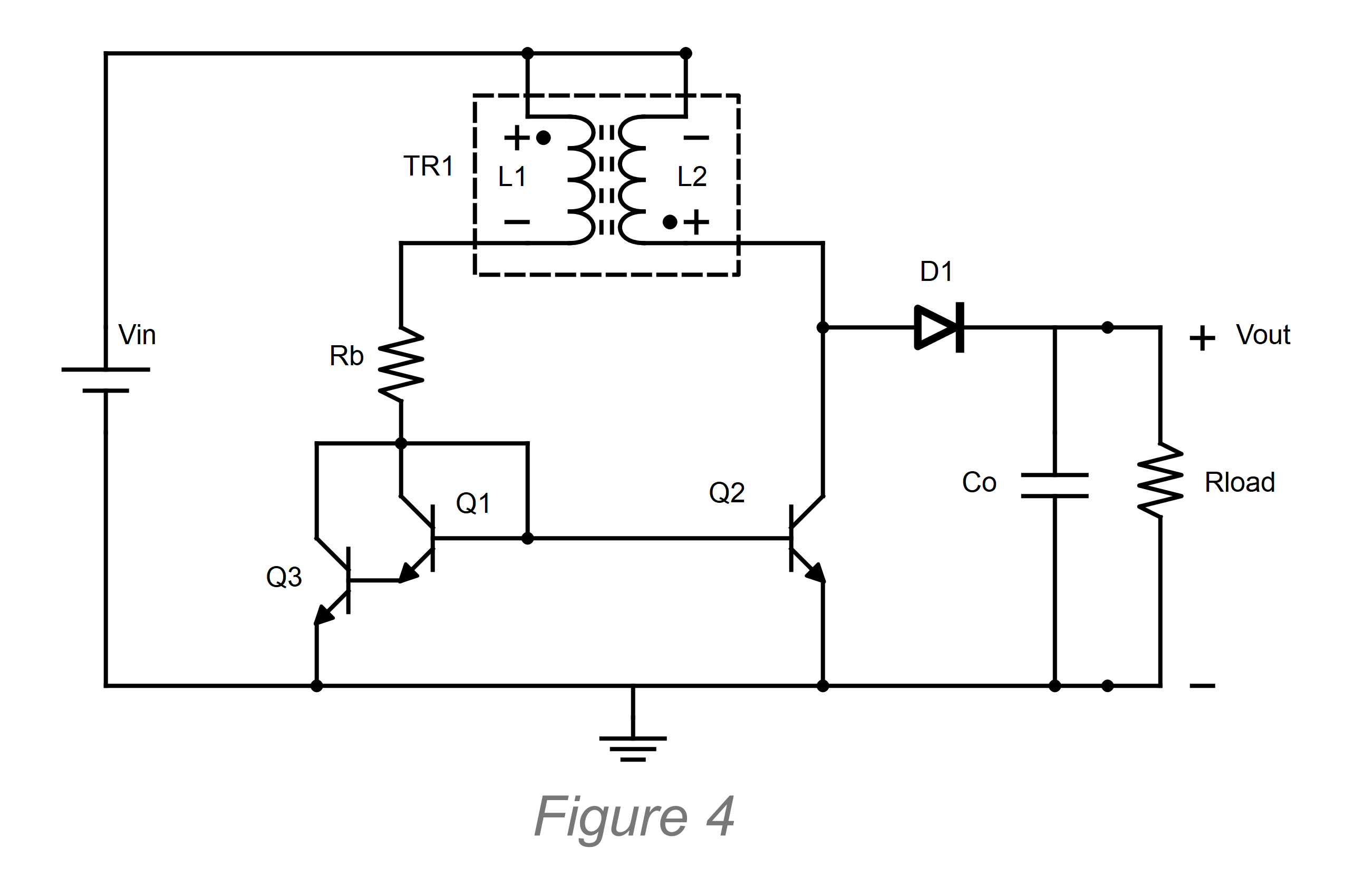
The circuit consists of a bipolar junction transistor current mirror connected to a transformer with inverted secondary coil, as shown in Fig. 4, forming a closed loop and generating positive feedback for voltage boosting. The current mirror transistor on the output side is driven by a pulse train and it determines the output voltage. The frequency of the pulses is largely determined by the transformer characteristics and the selected output objectives.
We will explore the potential of this topology to provide high output current and maintain a minimum output voltage for an extended period of time as the input voltage decreases due to gradual battery discharge.
|
Peak Efficiency |
~80% |
|
Minimum operational Vin -> Vout = 1.8 V |
0.45 V |
|
Iout for Vin of 1.5 V |
20 mA (max) |
|
Frequency for Vout = 1.8 V |
21.6 KHz |
|
Quiescent Current |
14 μA |
|
Output ripple |
< 10% |
[1] Andreas Tsiougkos, Vasilis F. Pavlidis, “A PWM-free DC-DC Boost Converter with 0.43 V Input for Extended Battery Use in IoT Applications”, 2021 IEEE International Midwest Symposium on Circuits and Systems (MWSCAS).
[2] A. Veerabathini and P. M. Furth, "A Low Output Voltage Ripple Fully-Integrated Switched-Capacitor DC-DC Converter," 2019 IEEE 62nd International Midwest Symposium on Circuits and Systems (MWSCAS).
[3] N. Tang, W. Hong, B. Nguyen, Z. Zhou, J. -H. Kim and D. Heo, "Fully Integrated Switched-Inductor-Capacitor Voltage Regulator With 0.82-A/mm2 Peak Current Density and 78% Peak Power Efficiency," in IEEE Journal of Solid-State Circuits, vol. 56, no. 6, pp. 1805-1815, June 2021
[4] N. Butzen and M. S. J. Steyaert, "Design of Soft-Charging Switched-Capacitor DC–DC Converters Using Stage Outphasing and Multiphase Soft-Charging," in IEEE Journal of Solid-State Circuits, vol. 52, no. 12, pp. 3132-3141, Dec. 2017
[5] R. Jain et al., "A 0.45–1 V Fully-Integrated Distributed Switched Capacitor DC-DC Converter with High Density MIM Capacitor in 22 nm Tri-Gate CMOS," in IEEE Journal of Solid-State Circuits, vol. 49, no. 4, pp. 917-927, April 2014
B. Eng. Kontogiannis Stefanos
M. Eng. Andreas Tsiougkos
B. Eng. Nikos Ladias
This project aims to evaluate a novel non-PWM boost converter for extending the battery life in IoT applications [1]. The proposed converter will be compared to a traditional PWM boost converter and a switched-capacitor boost converter. The purpose is to perform a comparative analysis between the non-PWM boost converter and the other state-of-the-art topologies [2]-[5] for a 1.5 V battery source scenario in order to demonstrate the significance and, possible, limitations of the non-PWM boost converter via the metrics of power efficiency, load regulation, and quiescent current.
power