MARMOT SOC
 Figure 1. MARMOT ASIC Chip Layout
Figure 1 shows the present chip layout of MARMOT SOC. Marmot ASIC contains core complex and peripheral complex logic. 0_ext_ram01, 0_ext_ram0h, 0_ext_ram1l, 0_ext_ram1h, 0_ext_ram2l, 0_ext_ram2h, 0_ext_ram3l, 0_ext_ram3h shows the I-Cache data arrays. t_ram01 and t_ram0h show tag RAM.

Figure 2. Block Diagram of Caravel and Rocket E31
Figure 2 shows a block diagram of MARMOT SOC. The Rocket SoC generator generated Verilog RV32IMAC RISC-V with 16KB I-Cache, and an array of peripherals. The Rocket SoC generated logic was designed to mate to the Caravel harness and I-Cache was mapped to OpenRAM. The 8KB part of I-Cache can be used as Instruction Tightly Integrated Memory (ITIM), a RAM showing up in the address map. ITIM can hold both instructions and data. The clock frequency seems limited to around 25MHz, slow but useful for many embedded applications. The Boot ROM implemented with logic gates jumps to the first address of SPI Flash. After that, a programmer can do what needs to be done executing from the program in SPI Flash. For example, change SPI Flash from the default Single SPI to Quad SPI and copy the routine to ITIM and jump to execution.
Why was the Rocket SoC Generator used in the first place?
Up to 70% of design and verification man-hours in chip design can be expended in connecting a CPU, QPI interface to flash memory, PSRAM, an array of UARTs, I2C and SPI in this case. Rocket SoC generator automatically generates a top level RTL derived from sub-circuit meta class definitions. Behind automatic SoC generation is the power of a new generation digital design language called Chisel. Chisel brings in software engineering, such as object-oriented and functional languages, into digital design. Chisel allows one to express hardware at the register-transfer level but allows one to write hardware generators.
Three Months with Rocket SoC Generator and OpenLane
Engineers kept day-time jobs and work took place after hours and weekends on and off. The month of February in 2022 had 28 days. First phase of project took exactly 30 days to obtain GDS. Second Chisel IP change took additional couple of months.
Feb 25, 2022: A decision was made to participate in multi-project wafer five (MPW-5)
Feb 26: MARMOT ASIC wish list was created.
Mar 16: Rocket SoC generation and logic simulation was complete. The OpenLane logic synthesis job threw an error in the middle.
Mar 17: One other engineer attempted to reproduce the error but ended up seeing varying errors. A conclusion was made that the error was caused by memory deprivation. Two new desktop PCs with 64GB RAM were hastily purchased.
Mar 19: OpenLane synthesis completed. Message shows the tool consumed 35GB of memory. Due to the scale of logic the Rocket SoC generator outputs and the way OpenLane logic synthesizer works, an excess of 35 GB of RAM was consumed. Several additional iterations were made to address the hold violations. Each run took 3 hours. OpenLane layout throws DRC errors.
Mar 20: Slack #openlane and GitHub Issue communities offered generous and articulate tips. DRC errors were suppressed. LVS errors in a similar fashion were resolved.
Mar 21: OpenLane routing tool threw “routing congestion” error but no further analytics. A way to get congestion area information was suggested but to no avail. The MPW-5 deadline mercilessly passed on Mar 22 in Japan time zone.
The following are the code changes: glue logic Verilog (350 lines) for Caravel terminal and I / O map: chip.scala, platform.scala; UART, I2C, SPI (100 lines): config.scala, system.scala
Mar 27: After trial and error, a GDS created. The design passed local precheck. Late for MPW-5 so move to ChipIgnite or MPW-6.
Apr 2: Regroup to design MPW-6. Decided to write Chisel for QPI PSRAM Interface mapped to CPU address space.
May 2: A PSRAM model was needed to simulate QPI interface. Obtained a model for "IoT DRAM" a fancy name for PSRAM with QPI. The model provided contained encrypted Verilog. The desinger had to move from Icarus to Modelsim Questa to run simulation.
May 29: Leveraging SiFive E300 Chisel code with the original specifications modified 400 lines in Chisel. The engineer only needed to correct the logical description part and was able to create a SPI IF and map PSRAM to memory. Synthesis and layout was repeated. Due to the fact that RAM is at the top 100 lines of Verilog was manually modified.
June 2: Project submitted.

Floor Plan and Automatic Routing
Initially an attempt was made to pack 16KB i$ and 16KB RAM like shown in the far left picture. The routing did not work. Then 16KB i$ and 8KB RAM were laid out as shown in the second picture from the left. Finally 16KB i$ only was the target spec settled in picture right. Placement of macrocell eventually led to the final laytout.

Figure 3. Floor Plan Evolution
Initial floor plan in the left of Figure 3 was made initially and evolved to middle, right and then Figure 1. While wiring clogs were anticipated we proceeded with the OpenLane digital design process but some wishes were removed as we made progress. This implementation was based on a “wish list.” The designer chose to droop wishes when only when it became crystal clear that a wish could not be granted.

Figure 4. MARMOT ASIC Wish List
Source: SiFive and University of California, Berkeley
A wish list was created. Wish list is frequently put to the side by management and engineers but believed to constitute a critical component of the project. Frequently original wishes include everything within itself and there are many possibilities. When the wishes descend on experts' minds, possibilities are few. Sometimes judgements interfere with perceptions.
Why an RTOS rather than a Linux?
 Figure 5. Linux IoT vs. RTOS IoT, Functions and Power Requirements
Figure 5 shows advantages and disadvantages of Linux IoT and RTOS IoT. Linux IoT offers more functions, a standardized programming environment, and consistent linear programming memory space to ease programming. RTOS systems are segmented into multiple microcontrollers which complicates programming the device. On the other hand RTOS IoT may turn off parts of the systems not being used at the time. Linux IoT may hibernate but DRAM refresh draws power even when the system is hibernating.
 Figure 6. An IoT system example MARMOT ASIC is to be applied
Figure 6 shows an example IoT system. Endpoint and Gateway operate on a solar panel for years of duration untethered from permanent power supply.
IoT Power Supply Unit

Figure 7. Power supply unit (PSU) example for RTOS IoT
A power supply unit (PSU) in Figure 7 receives power from multiple sources e.g. solar, lithium-ion, variable DC voltage (e.g. 2.6V-20V), and USB-C. The PSU supplies 7 independent power rails, 6 of which can be turned on and off using I2C commands. The PSU is capable of measuring current flow in each of its power rails while the IoT is in operation. The measurement circuit was designed not to cause significant power loss when current measurement is not made. An IoT service provider needs to know when its IoT device is tampered, cloned, implanted. A remote power analysis of its IoT device can reveal some physical, structural and electrical breaches of the device such as cloning, implant, and malware.
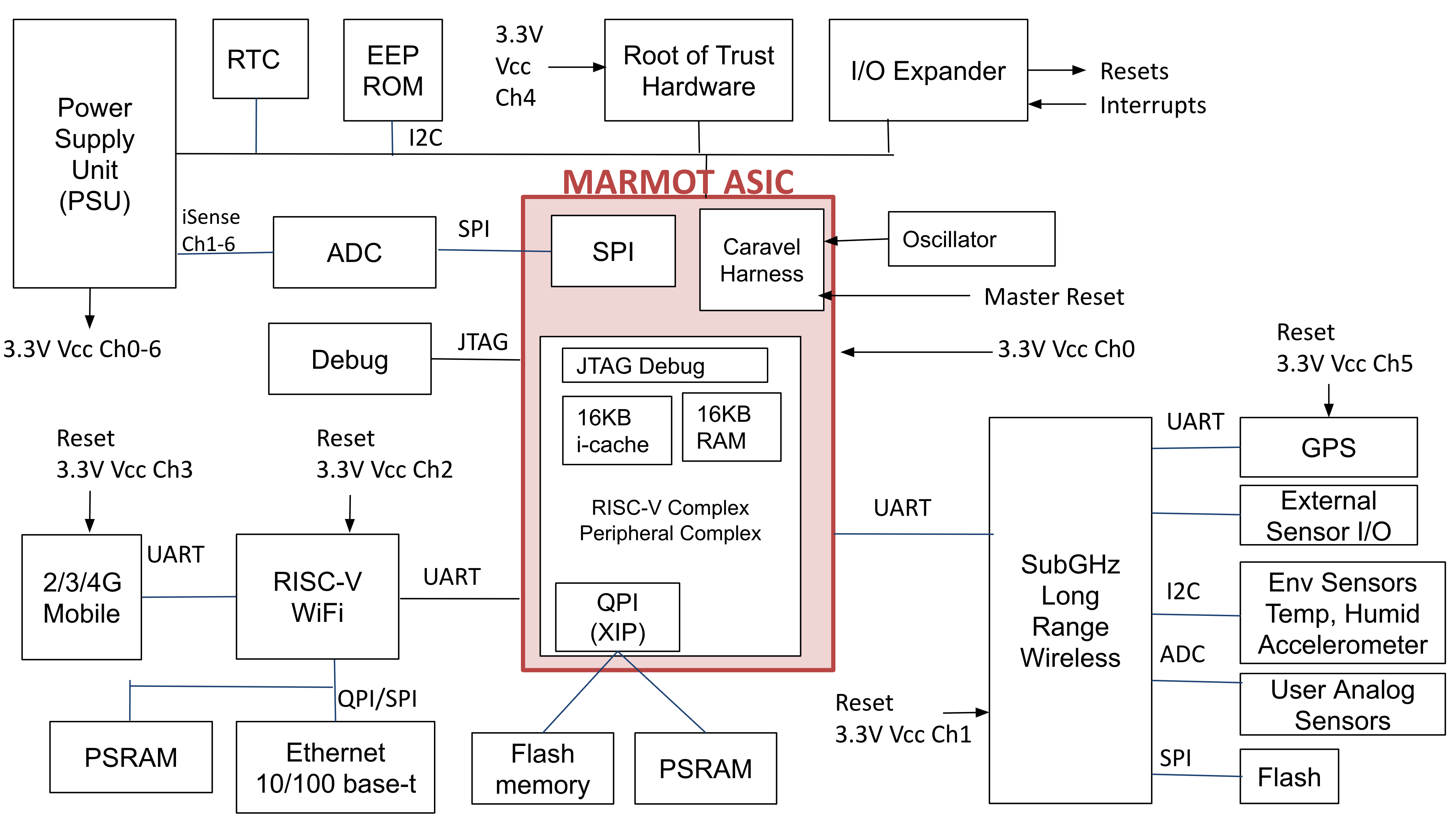
Figure 8. RTOS IoT Power Rails in Block Diagram
Figure 8 shows an example system to which MARMOT ASIC is integrated with power rail descriptions. A discrete ADC achieves a higher sample rate than a standard microcontroller. Large sample data captured is stored in PSRAM e.g. 16MB.General purpose input and output (GPIOs) are expanded for crisscrossing reset and interrupt pins.
 Figure 9. A Picture of an RTOS IoT
Figure 9 shows an example system for MARMOT ASIC. Please note multiple wireless chipsets. These chips are connected to each other via UARTs for data / control exchanges. The UARTs are used not only for IoT applications but also for over-the-air firmware upgrade (OTA). I2Cs are needed to interface sensors and root-of-trust (RoT) hardware.
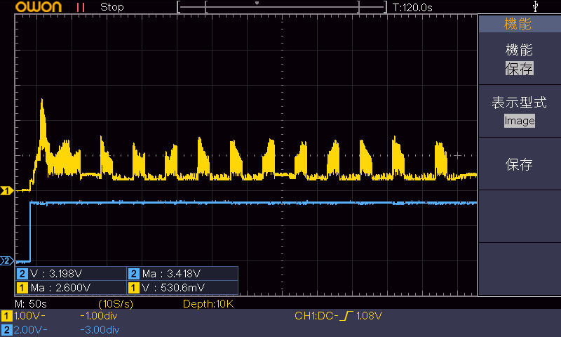
Figure 10. Icc and Vcc waveforms for 2G/3G/4G-LTE power rail
Figure 10 shows example waveforms from a power line, current in yellow and voltage in blue, in this case from a LTE wireless chipset. After turning on the power and initialization process is complete, the processing that consumes power is performed every 30 seconds.
Conclusions
The idea of combining a Rocket SoC generator with an ASIC that leverages a Caravel harness to develop a practical microcontroller ASIC using a 130 nanometer Sky130 process seemed good from the beginning. I still think so after a month. The technical approach requires more lengthy scrutiny. I think I will spend a lot of time clarifying what can be embodied from the technology of open source EDA tools and process development kits. Even if Moore's Law disappears, semiconductor digital circuits can be dramatically miniaturized, and semiconductors still provide much higher reliability than PC boards. By giving system manufacturers the ability to design microcontroller ASICs almost with very little capital investmnet, the open source EDA tools, PDK and IPs bring tons of future potential competitiveness to their business. Furthermore the legacy semiconductor fabs that exist in all all over the world not only survive, but they will have great business potential in the future.
Acknowledgements
This work is based on results obtained from project, JPNP16007, commissioned by The New Energy and Industrial Technology Development Organization (NEDO).

Targeting 5-year continuous operation, a solar panel, a power supply board, a logic board, and lithium batteries are to be integrated in a waterproof housing to form an IoT. The power supply board controls the solar, lithium-ion battery, and system power supply, and measures the power consumption. Evaluation boards were produced in December, 2021, and characterized in March, 2022. We created a breadboard for circuit verification of logic board. In March 2022, functions of secure MCU, sensor cloud communication, and OTA were verified. A custom board design will start in June, 2022. A RISC-V ASIC (CSP60), a part of security function, will be prototyped using Google's free shuttle. The GDS layout was completed in March, 2022. ber of the same year, the ASIC will be integrated into the logic board on the flexible board.
processor
sky130A