The design of monolithic radio-frequency integrated circuits (RFICs) is a multidisciplinary project that spans from microelectronics to electromagnetics. So, naturally, the design flow of an RFIC uses different pieces of software for different parts of the process. This process, if done in an industry-standard environment, requires a number of (expensive) licenses for proprietary software and simulators - from SPICE to Full-Wave solvers to parasitics extractors - as well as an NDA that grants use to a process design kit of a certain technology... all this is out of reach of someone who's not an employee of a design house or a researcher in academia.
But all is not lost, not lost indeed, because now there is an open-source PDK available: the Skywater 130nm CMOS process was released to the public and every detail of the technology is accessible to the curious, no NDA needed. This is huge. This means that anyone with access to some EDA tools could design their own integrated circuits, including the hobbyist community, small design houses and small research groups.
The PDK also comes with suggestions of open-source, free tools that can be used to create a working design flow for digital and analog designs. These tools cover all of the needs of a digital circuit synthesis and most of the needs of the analog circuit design flow. The RFIC design flow shares some tools with the analog circuit flow, but there are some areas, especially in Full-Wave solvers and parasitic extraction, that need some more attention.
Having these needs in mind, and knowing that the 130nm CMOS node can be useful for RF circuits at least up until the 60 GHz ISM band, we have decided to build a demonstrator chip for 60 GHz applications. This chip doesn't aim to be a high-performer, nor to adhere to commercial standards and specifications, but instead it aims to serve as a proof-of-concept: to prove that, if done correctly, a complete open-source RFIC design flow on a low-cost CMOS technology could produce useful designs.
The submission will include a Voltage Controlled Oscillator (VCO), a Power Amplifier (PA), a Low Noise Amplifier (LNA), a Variable Gain Amplifier (VGA) a Detector, a Balun, a microstrip plus SCPW set, plus a TRL kit for de-embedding. The expected performance of these circuits, as well as their basic schematic, are presented below:
VCO: Cross-coupled pair-based VCO with source-follower buffers and a resonant tank based on a planar inductor and differential varactor bank for frequency tuning. CCP biasing done by a 1:1 current mirror to improve matching of the reference and core currents. Expected results: 3 GHz tuning range at 60 GHz, phase noise better than -100 dBc/Hz at 10 MHz offset from the carrier frequency at 18 mW of DC power consumption (VCO core only), maximum DC power consumption of 36 mW. Buffer with input capacitance smaller than 6 fF, output reflection loss smaller than 10 dB inside the V-band.

VGA: Standard cell implemented with a cascode with current-steering technique to implement power gain tuning. The amplifier standard-cell load is implemented with microstrip stubs. The cells are cascaded to realize the needed maximum gain. The amplifier will operate in class A.
Maximum gain of 10 dB, gain control range better than 20 dB (from -10 dB to +10 dB), 10dB input and output bandwidth of 15% centered at 60 GHz (from 55.5 GHz to 64.5 GHz). Typical DC power consumption of 20 mW per cell, maximum of 40 mW. Output 1dB compression point of -20 dBm. Source paper: DOI 10.1109/LMWC.2014.2316253.

Microstrips and SCPW: DUTs include a 1mm-long, 50-ohm microstrip line and a 1mm-long, 50-ohm slow-save CPW (SCPW). TRL structures include a the GSG pads, the through, an open-circuit reflect and a lambda/4 line centered at 60GHz.
Expected results: attenuation constant lower than 2 dB/mm for the microstrip, lower than 1.5 dB/mm for the SCPW.
PA:
The power amplifier will use a multi-stage topology to simplify the design procedure, as it is a proven and standard PA design. The drain load could be implemented with planar inductors instead of microstrips to simplify the design, as well as the input and output matching networks, if needed.

Expected results:
|
Parameter |
Typical |
|
Total current consumption |
30 mA |
|
Operating Frequency |
60 GHz |
|
Input impedance |
50 |
|
Output impedance |
50 |
|
Input Return Loss |
< 10 dB |
|
Output Return Loss |
< 10 dB |
|
Banwidth |
9 GHz |
|
1dB compression Point |
6 dBm |
LNA: A cascode with tuned LC load for narrow-band amplification, including source degeneration to match the noise impedance of the circuit. The circuit includes input and output impedance-matching networks. The amplifier will operate in class A.

Expected results:
|
Parameter |
Condition |
Minimum |
Typical |
Maximum |
|
Total current consumption |
|
|
20 mA |
40 mA |
|
Operating Frequency |
20 MHz of BW |
59.99 GHz |
60 GHz |
60.01 GHz |
|
Input impedance |
@ 60 GHz |
50 |
50 |
55 |
|
Output impedance |
@ 60 GHz |
- |
50 |
|
|
Input Return Loss |
S11 @ 60 GHz |
- |
- |
-24 dB |
|
Noise Figure |
@ 60 GHz |
- |
3 dB |
- |
|
Inter-modulation product |
Third Order Intercept Point Ref. to 50 ohms |
-10 dB |
- |
- |
|
Compression Point* |
compression (referred to 50 ohms) |
-20 dB |
- |
- |
|
Input power accepted |
@ 60 GHz |
|
-84 dBm |
|
Detector: The detector will be implemented as a traditional MOSFET detector circuit, where the FET implements the high-speed rectification element. The necessary passive elements, Ib and the shunting capacitor C, will be implemented with a current mirror and a MIM capacitor, respectively.

Reference article: 10.1109/IMS30576.2020.9223863.
The specifications below are for the entire 60 GHz ISM band (57-66 GHz).
|
Sensitivity |
10 V/mW (linear) |
|
Sensitivity Flatness over Freq. Band |
+-4 dB |
|
Minimum Detection Power |
-50 dBm |
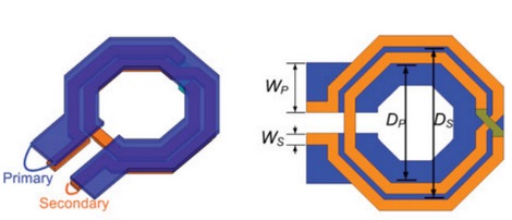
Balun: Our goal is to build two balanced to unbalanced transformers, differing from each other by the transformation ratio: one 1:1 (no transformation ratio) and the other 1:n, where 'n' is the highest value obtained respecting the metal density design rule. As shown in the article from which the figure below is taken, changing the metal width of the coils separately has the effect of changing this 'n'. This will help us to estimate, for future device layouts, the possible values of the transform ratio and the signal insertion loss, which is a function of the shape, structure and materials used for its manufacture.
doi:10.1017/S1759078711001073
The specifications below are for the entire 60 GHz ISM band (57-66 GHz).
|
Parameter |
1:1 |
1:n |
|
Insertion Loss (S21, S31) |
-6 dB |
n-dependent |
|
Return Loss (all ports) |
< -10 dB |
< -10 dB |
|
Nominal Phase Shift (between outputs) |
180 degrees |
180 degrees |
|
Common Mode Rejection |
> 20 dB |
> 20dB |
|
Amplitude Balance (between outputs) |
< 2 dB |
< 2 dB |
Team members:
Leader: Leonardo Amorese Gallo Gomes, PhD candidate at University of São Paulo (Brazil) and Communauté Université Grenoble-Alpes (France). E-mail: amorese.leonardo@gmail.com, leonardo.gomes@usp.br
João Eduardo Gentil Lé, master student at Univesity of São Paulo (Brazil). E-mail: joao.le@usp.br, joao.le@tutanota.com.
Walter Santiago Campos Aranda, Master degree student at University of São Paulo (Brazil). E-mail: walter.aranda@usp.br, camposaranda@gmail.com
Luis Antonio Quispe Cartagena, PhD student at Univesity of São Paulo (Brazil). E-mail: lcartagena@usp.br
The goal is to build a demonstrator chip in the 10 mm² user project area to assess the feasibility of implementing mm-wave designs in a low-cost technology using a complete open-source RFIC design flow. We propose to submit a number of basic mm-wave circuits, such as voltage-controlled oscillator, power amplifier, balun, low-noise amplifier and detector, as well as some test features like inductors, (slow-wave) transmission lines and a basic TRL calibration kit.